

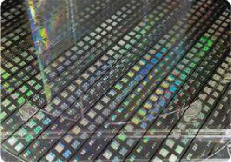
As electronics continue to shrink and increase in complexity, conventional optics remain limited by traditional glass and plastic manufacturing. MetaOptics was founded to bridge this gap by combining semiconductor-grade fabrication with advanced optical design, enabling wafer-level metalens that are ultra-thin, scalable, and production-ready. Achieving reliable performance at sub-wavelength scales requires physics-accurate simulation to model light–matter interaction and translate nanoscale behavior into predictable, system-level optical performance.
From its early stages, MetaOptics recognized the importance of a strong simulation foundation and engaged with CADFEM SEA for initial consultation on simulation software strategy and supporting hardware requirements, ensuring a scalable and future-ready engineering environment.
Company Description
MetaOptics is a technology company focused on advancing metalens innovation through a combination of precision optical design and scalable manufacturing. By developing its own manufacturing, testing, and assembly capabilities, MetaOptics enables reliable integration of metalens solutions across consumer electronics, sensing, and imaging applications. Driven by continuous innovation and engineering excellence, the company aims to establish itself as a global leader and center of excellence in metalens technology.
Business Challenges
MetaOptics' goal was not to demonstrate laboratory concepts, but to deliver metalens-based products that could be manufactured reliably at scale.
- Designing ultra-thin metalenses capable of high image quality across RGB wavelengths and wide fields of view, while controlling chromatic aberrations and off-axis distortions.
- Nanoscale variations in fabrication—such as lithography deviations, misalignment, and material changes—could significantly impact optical performance if not addressed early.
- Translating electromagnetic behavior at the nanoscale into predictable system-level metrics such as MTF, signal-to-noise ratio, and sensor coupling.
- Ensuring designs were compatible with high-throughput semiconductor processes, rather than limited to small-batch prototyping.
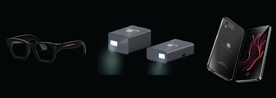
- Supporting multiple product lines—including cameras, biometric sensors, and picoprojectors—within constrained development schedules
Engineering Solutions
To overcome these challenges, MetaOptics implemented a simulation-driven design workflow integrating Ansys Lumerical and OpticStudio, enabling tight coupling between physics-based modeling and system-level validation.
- High-fidelity simulations captured broadband, angular, and polarization behavior of metalens nanostructures, forming a reliable foundation for optical design.
- Manufacturing and assembly variations were modeled early, allowing MetaOptics to identify robust designs resilient to real-world process deviations.
- Electromagnetic results were translated into system-level optical models, enabling accurate prediction of imaging performance in realistic product environments.
- Optical performance was evaluated in the context of mechanical alignment and module packaging, helping define realistic assembly tolerances.
Benefits
By embedding simulation at the core of its engineering process, MetaOptics achieved measurable technical and commercial gains:
- Early virtual validation significantly lowered the need for physical redesigns, accelerating time from concept to validated prototype.
- Designs optimized for manufacturing variability showed stronger correlation between simulated and fabricated performance.
- End-to-end simulation of optical modules reduced downstream validation risk and increased confidence at product launch.
- Simulation-enabled workflows supported rapid development of metalens-based cameras, biometric sensors, and imaging modules.
- A robust, simulation-backed design process strengthened MetaOptics' position as a scalable technology leader, supporting investor confidence and its public listing on the Singapore Exchange Catalist board.
"Integrating Ansys simulation into our workflow with CADFEM's support has allowed us to design metalens systems that are not only high-performance in theory but manufacturable and predictable in real production environments. This capability was crucial in bringing our own color cameras, mobile phone modules, picoprojectors, biometric sensors, and wide-FoV imaging products to market readiness efficiently.